


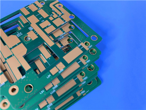

Высокочастотный гибридный сбор: проектирование 8-слойной доски с RO4350B, FR-4 и последовательной ламинировкой
Контактное лицо : Sally Mao
Номер телефона : 86-755-27374847
Ватсап : +8618277967574
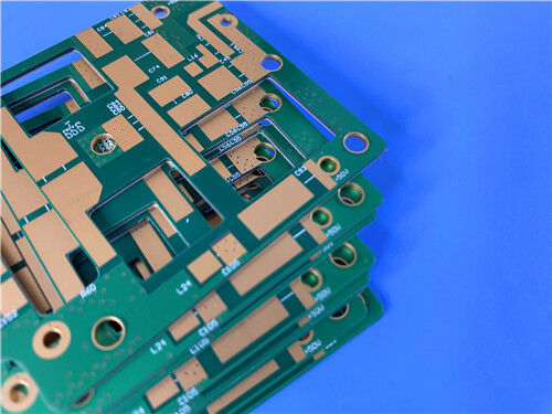
| Количество мин заказа : | 1 шт. | Цена : | 0.99USD/PCS |
|---|---|---|---|
| Упаковывая детали : | упаковка | Время доставки : | 2-10 рабочих дней |
| Условия оплаты : | Т/Т, ПайПал | Поставка способности : | 50000 шт. |
| Место происхождения: | Китай | Фирменное наименование: | Panasonic |
|---|---|---|---|
| Сертификация: | ISO9001 | Номер модели: | М6 |
Характер продукции
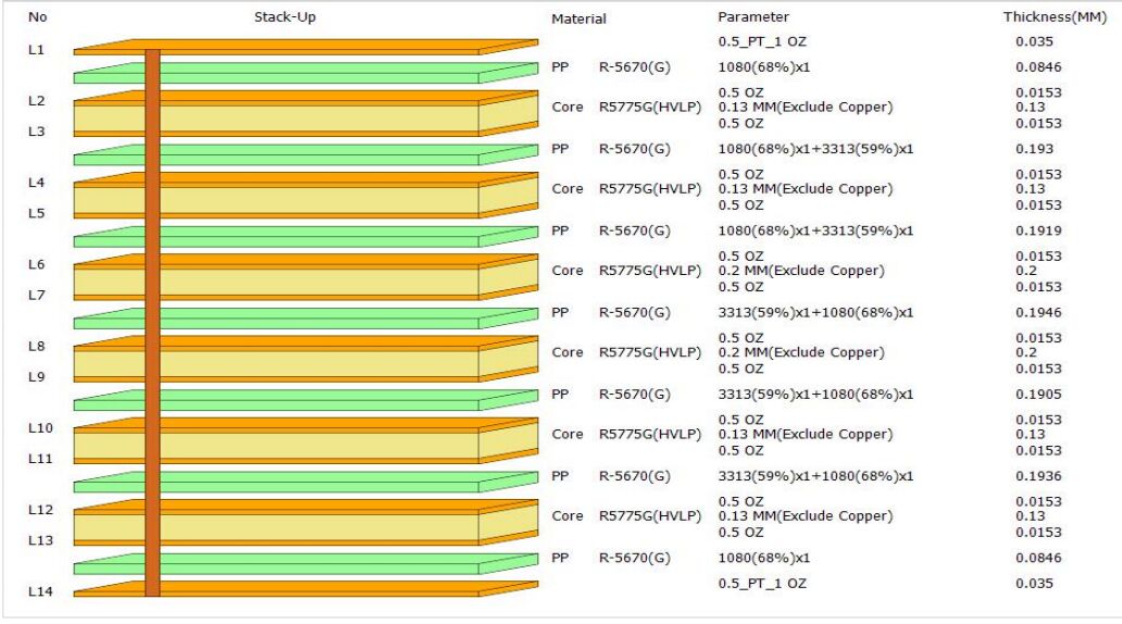
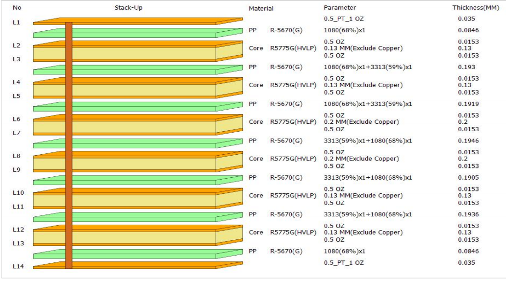
14-слойный ПКБ M6 с многоточечным контролем импеданции
По мере того как скорость передачи данных выходит за рамки 25 Гбит/с и переходит в область 56G и 112G PAM4, обычные материалы для печатных плат, такие как стандарт FR-4, достигают своих практических пределов.и выбор ламинированного материала напрямую определяет успех или неудачу высокоскоростного проекта.В этой статье рассматривается сложная 14-слойная плата, построенная на материале M6, с строгим контролем импеданса в пяти критических точках, надежностью класса IPC-3,и передовые методы обработки.
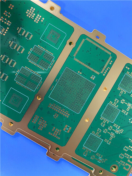
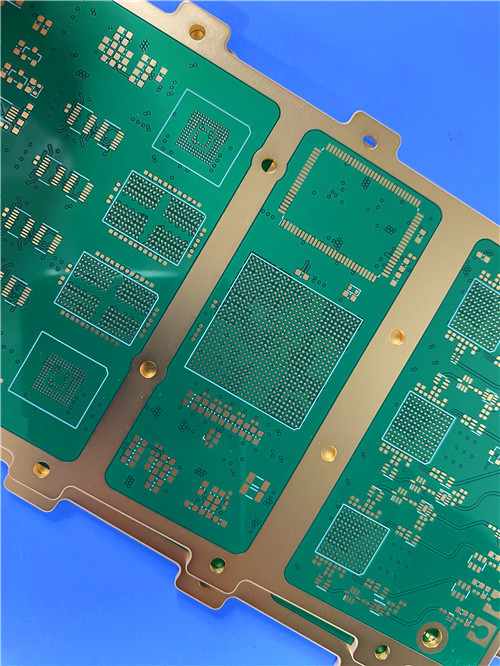
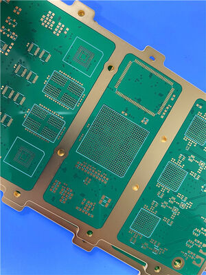
Снимок продукта: 14-слойная высокоскоростная плата
Количество слоев: 14 слоев
Базовый материал: серия M6 (Ламинат R-5775 ((N), Prepreg R-5670 ((N))
Толщина доски: 2,406 мм
Медь Вес: Внутренние слои 0,5 унции готовой меди, внешние слои 1 унции готовой меди
Маска для сварки: зеленый с белыми буквами
Поверхностная отделка: никель-палладий-золото (ENEPIG)
Размер панели: 106 мм х 102 мм = 1 часть
Стандарт качества: класс IPC-3 (высокая надежность)
Управление импеданцией: 5 пар дифференциалов, каждая из которых регулируется до 100Ω ± 10%
Пробелы: диаметр 0,2 мм, забитые смолой, электропокрытые для сглаживания поверхности
Что такое M6 Board Material?
M6 представляет собой высокоскоростной ламинированный материал с низкими потерями из серии Megtron, специально разработанный для применений, требующих превосходной целостности сигнала на высоких частотах.
Оба классифицируются как "Многослойные материалы с высокой скоростью и низкими потерями" с низкой конструкцией стеклянной ткани Dk, которая уменьшает задержку распространения сигнала и улучшает консистенцию импеданса.
Таблица ключевых параметров (от R-5775 ((N) Datasheet)
| Недвижимость | Условия испытания | Типичная стоимость |
| Температура преобразования стекла (Tg) DSC | Как получено | 185°C |
| Температура преобразования стекла (Tg) DMA | Как получено | 210°С |
| Температура термического разложения (Td) | TGA | 410°C |
| Время в Делам (T288) без Cu | – | > 120 мин |
| Время для Делама (T288) | – | > 120 мин |
| CTE (ось Z, α1) | < Tg | 45 ppm/°C |
| Диэлектрическая константа (Dk) ?? @ 1 ГГц | С-24/23/50 | 3.4 |
| Диэлектрическая константа (Dk) ?? @ 13 ГГц | IEC 63185 | 3.34 |
| Коэффициент рассеивания (Df) ?? @ 1 ГГц | IPC 2.5.5.9 | 0.002 |
| Фактор рассеивания (Df) @ 13 ГГц | IEC 63185 | 0.0037 |
| Сопротивляемость объема | C-96/35/90 - Процесс рассмотрения | 1 × 10⁹ МΩ·см |
| Сопротивляемость поверхности | C-96/35/90 - Процесс рассмотрения | 1 × 10⁸ МΩ |
| Поглощение воды | D-24/23 | 0.14% |
| Устойчивость к очистке (1 унция фольги H-VLP) | Как получено | 00,8 кН/м |
| Возгораемость | UL94 | V-0 |
M6 Варианты материалов (типы ядра)
M6 доступен в нескольких толщинах ядра, каждая из которых имеет определенный стиль стеклянной ткани и содержание смолы:
| Тип ядра | Фактическая толщина (мм) | Стиль стеклянной ткани | Содержание смолы (%) | Dk @ 1 ГГц | Df @ 1 ГГц |
| Тип 2 | 0.05 | 1035 | 67 | 3.25 | 0.002 |
| Тип 4 | 0.1 | 2013 | 56 | 3.4 | 0.002 |
| Тип 5 | 0.125 | 2116 | 56 | 3.4 | 0.002 |
| Тип 8 | 0.2 | 2013 | 56 | 3.4 | 0.002 |
| Тип 10 | 0.25 | 2116 | 56 | 3.4 | 0.002 |
| Тип 30 | 0.75 | 2116 | 56 | 3.4 | 0.002 |
Области применения M6
Высокопроизводительные вычисления (серверы, коммутаторы, маршрутизаторы)
Оптические приемопередатчики (400G, 800G)
Телекоммуникационная инфраструктура (базовые станции 5G, обратная связь)
Оборудование для испытаний и измерений
Аэрокосмическая и оборонная промышленность (радар, электронная война)
Ключевые пункты обработки для M6
На основании руководящих принципов процесса M6 производители должны обращать внимание на:
Хранение: Препрег R-5670 следует хранить при температуре ≤23°C и ≤50% RH. Для длительного хранения требуется 5°C. Открытые пакеты должны быть запечатаны; совокупное воздействие не должно превышать 8 часов.
Обработка с соединением внутреннего слоя: приемлемо использование черного/коричневого оксида, но предпочтительна альтернативная обработка оксидом (технология пероксида/серного нанесения).После обработки оксидом рекомендуется выпечь на стойке при температуре 105 °C в течение 20-30 минут..
Сверление: используйте высокоугольные винтовые буровые винты и смазанные входные листы (например, LE-листы).Нагрузка на чип 20 мкм/св.3000 просмотров.
Для перманганатного дезмея рекомендуется дважды больше времени, чем для FR-4. Для плазменного дезмея рекомендуется половина времени, чем для FR-4.Для гибридных конструкций с FR-4, рекомендуется комбинированный процесс (плазменный период полураспада + перманганат без опухоли).
ENIG Предупреждения: при использовании ENIG (как и данный продукт) необходимо выпечь его при температуре 150°C в течение 5 часов или хранить при комнатной температуре в течение 1 недели перед никелированием, чтобы предотвратить дефекты покрытия.
Ламинация: скорость нагрева: 2,0-4,0°C/мин. Давление: 3,0-4,0 МПа. Температура продукта должна превышать 185°C в течение 75 минут.
Типы импеданции
Контроль импедантности - это практика сопоставления характеристической импедантности линии передачи с источником и импеданциями нагрузки для минимизации отражения сигнала.пять пар дифференциалов регулируются до 100Ω ± 10%Давайте рассмотрим ключевые типы импеданс и как они применяются.
Одностороннее сопротивление
Один проводник, ссылающийся на наземную плоскость (обычно на соседнем слое). Общие значения: 50Ω или 75Ω. Используется для отдельных сигналов, таких как часы, радиочастотные пути или одноконтактные линии передачи данных.
Дифференциальное сопротивление
Это тип, используемый в текущем продукте. Два совпадающих следа, несущие равные и противоположные сигналы. Дифференциальное импеданс - это импеданс между двумя следами.Стандартное значение для высокоскоростных дифференциальных пар (USB), PCIe, Ethernet, LVDS) составляет 100Ω.
Почему 100Ω дифференциал?Это значение балансирует потребление энергии, шумоподавляемость и совместимость со стандартными конструкциями приемопередатчиков.
Копланарное сопротивление
Следы соотносятся с земными плоскостями на том же слое (через прилегающие земли) в дополнение к базовой плоскости ниже. Это обеспечивает лучшую изоляцию и более строгий контроль,часто используется в RF-конструкциях или когда расстояние между слоями несовместимо.
Микрострип против Стриплайн
| Структура | Описание | Преимущества | Недостатки |
| Микроштрипы | Следование внешнего слоя с одной базовой плоскостью ниже | Легче изготовить, меньше потерь, доступно для исследования | Более восприимчивы к перекрестному прослушиванию и EMI |
| Стреловая линия | Следование внутреннего слоя с базовыми плоскостями выше И ниже | Отличная ЭМИ защита, симметричное поле, постоянная импеданс | Более высокие потери, труднее изготовить, медленнее распространение |
Импедантные конструкции в данном продукте
Из таблицы с расчетами импеданса мы можем определить две различные структуры:
1. Крайне-сцепленная покрытая микрополоска 1B (импеданс 1 & 2 L1 и L14)
2. Оффсетная линия 1B1A с краевой сцепкой (импеданс 3, 4, 5 ¢ L5, L10, L12)
Зачем пять точек контроля импеданции?
Пять управляемых пар дифференциалов (L1, L14, L5, L10, L12) отражают сложность высокоскоростного маршрутизации:
L1 и L14 (внешние слои): вероятно, для сигналов, которые должны входить/выходить из платы без проводов, или для точек испытания.
L5, L10, L12 (внутренние слои): Структуры стриплайн для длинных высокоскоростных путей, требующих максимальной защиты от EMI и постоянного импеданса на больших расстояниях.
Диэлектрическая высота каждого слоя (H1/H2) и Dk (Er1/Er2) различаются из-за свертывания, что требует независимой регулировки ширины следа (W) и расстояния (S) точно так, как показано в графах "Правильно".
Дополнительные характеристики надежности
Ключевые требования включают:
100% электрическое испытание на непрерывность и изоляцию
Требования к более жесткому кольцевому кольцу (не менее 50% прокладки)
Более строгое качество стенки отверстия (без пустоты, без трещин после теплового напряжения)
Полное заполнение покрытых отверстий (без пустоты в меди)
0.2 мм проемы: смоловая прокладка + электропластировка гладкости
Небольшие сквозняки (0,2 мм в диаметре) являются стандартными для конструкций с высокой плотностью.
Однако, открытые каналы могут вызывать проблемы:
Сварка сварки во время сборки
Застрявший поток, вызывающий выброс газов
Неравномерная поверхность для размещения компонентов
Электропластировка (покрытие крышкой) затем пластины меди над пробкой, создавая плоскую, плоскую поверхность.
Это позволяет:
Дизайн с прокладкой в прокладке (прокладки, расположенные непосредственно под прокладками BGA)
Улучшенная надежность (без пустоты, без загрязнителей)
Улучшенное рассеивание тепла (твердый медный колпачок)
Заключение
Этот 14-слойный M6 PCB представляет собой современное высокоскоростное цифровое проектирование.Класс надежности IPC-3, и продвинутый с помощью обработки (зашивка смолой + электропластировка сглаживания), плата специально разработана для приложений, требующих целостности сигнала на 25+ Гбит / с.
Использование как микрополосы (L1, L14) и офсетные строки (L5, L10, L12) демонстрирует сложное понимание управления импедансом в различных типах слоев.Для инженеров, специфицирующих аналогичные платы, внимание к хранению материала, параметрам бурения, циклам размазки и предварительной печи ENIG (как описано в Руководстве по процессу M6) имеет важное значение для достижения успеха первого прохода.
Впишите ваше сообщение

RO4350B, 4003C; Rogers 5880, 5870, 6002, 6010, 6006, 6035; RO3003, RO3035, RO3006, RO3010, RO3210, RO3203
TLX-8, TLX-6, TLX-9, TLX-0, TLX-7, TLY-3, TLY-5, RF-35TC, RF-60TC, RF-35A2, RF-60A, AD450, AD600, TMM4, TC350
| Shenzhen Bicheng Electronics Technology Co., Ltd |
| городок 6-11К Шидай Джингюан Фуйонг, район Баоан, город Шэньчжэня, провинция Гуандун, Китай |
| 86-755-27374946 |
| sales30@bichengpcb.com |