



RO3006 Высокочастотный ПХБ-ламинированный: Dk 6.15, Низкие потери и CTE, сопоставленные с меди для компактных RF-конструкций
Контактное лицо : Sally Mao
Номер телефона : 86-755-27374847
Ватсап : +8618277967574
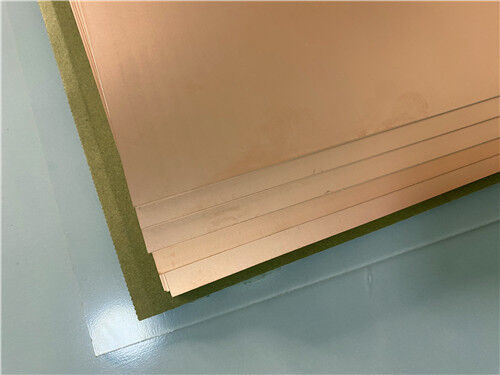
| Фирменное наименование: | Rogers | Номер модели: | TMM10i |
|---|
Характер продукции
Это термореактивный микроволновый ламинат с керамическим наполнителем, производимый компанией Rogers Corporation. Он входит в серию TMM®. Диэлектрическая проницаемость (Dk) составляет 9,80 ±0,245 при 10 ГГц. Тангенс угла диэлектрических потерь (Df) составляет 0,0020 при 10 ГГц. Материал имеет изотропную диэлектрическую проницаемость. Коэффициент теплового расширения (CTE) составляет 19 ppm/°C во всех направлениях (X, Y и Z). Это соответствует CTE меди. Температура разложения (Td) составляет 425°C. Теплопроводность составляет 0,76 Вт/(м·К). Материал представляет собой термореактивную смолу. Он не размягчается при нагревании. Возможно выполнение проволочной сварки без опасений отслоения контактных площадок или деформации подложки. Обработка нафтанатом натрия перед химическим осаждением не требуется.
Какие печатные платы можно изготовить с его помощью?
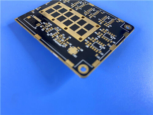
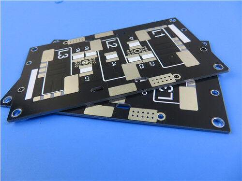
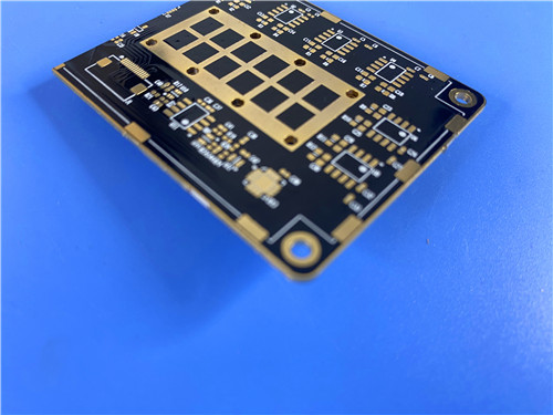
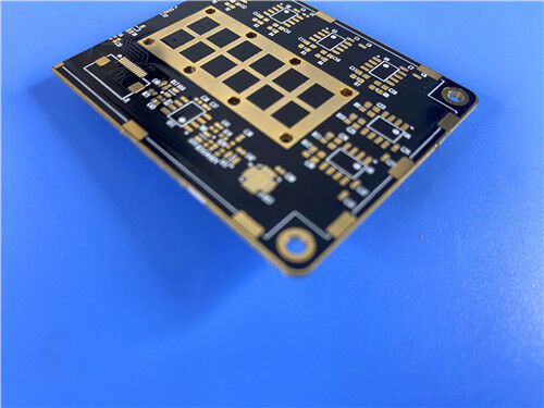
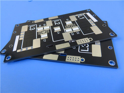
Может быть предложено комплексное 2-слойное решение для ВЧ печатных плат. Плата основана на материале TMM10i. Готовая толщина составляет 0,8 мм. Толщина меди составляет 1 унция на слой. В качестве финишного покрытия применяется ENIG (химический никель/иммерсионное золото). Черная паяльная маска нанесена с обеих сторон. Белый шелкотрафарет напечатан с обеих сторон. Применено краевое покрытие. Минимальная ширина проводника и зазор составляют 6 и 9 мил соответственно. Минимальный размер отверстия составляет 0,4 мм. Толщина металлизации переходных отверстий составляет 20 µм. Стандарт качества - IPC Class 2. Эта плата идеально подходит для ВЧ/СВЧ схем, усилителей мощности, фильтров, спутниковых систем связи, антенн GPS и тестеров микросхем.
1. Обзор материала
TMM10i - это термореактивный микроволновый материал. Он производится компанией Rogers Corporation. Он входит в серию TMM®. Это композитный полимер на основе углеводородной термореактивной смолы с керамическим наполнителем. Он разработан для высокой надежности металлизированных отверстий. Он подходит для применения в стриплайновых и микрополосковых линиях.
Серия TMM сочетает в себе многие желаемые свойства керамических подложек с простотой технологий обработки мягких подложек. Она не требует специализированных производственных технологий. Она не требует обработки нафтанатом натрия перед химическим осаждением. Это снижает сложность и стоимость изготовления.
Ключевые особенности TMM10i:
Изотропная диэлектрическая проницаемость— Dk одинакова во всех направлениях. Это упрощает проектирование и обеспечивает стабильную работу.
Высокая диэлектрическая проницаемость— Dk составляет 9,80 ±0,245. Это позволяет достичь меньших размеров схем.
Низкий тангенс угла диэлектрических потерь— Df составляет 0,0020 при 10 ГГц. Потери сигнала минимизируются.
CTE, соответствующий меди— CTE составляет 19 ppm/°C во всех направлениях. Это соответствует CTE меди. Обеспечивается превосходная стабильность размеров. Гарантируется высокая надежность металлизированных отверстий.
Термореактивная смола— Материал не размягчается при нагревании. Возможно выполнение проволочной сварки без опасений отслоения контактных площадок или деформации подложки.
Теплопроводность— Теплопроводность составляет 0,76 Вт/(м·К). Это примерно в два раза больше, чем у традиционных ламинатов PTFE/керамика. Облегчается отвод тепла.
Химическая стойкость— Материал устойчив к травителям и растворителям. Могут использоваться все распространенные процессы изготовления печатных плат.
Стойкость к ползучести и холодному течению— Механические свойства устойчивы к ползучести и холодному течению. Стабильность размеров сохраняется с течением времени.
2. Техническая спецификация TMM10i
| Свойство | Типичное значение | Направление | Единицы измерения | Условие | Метод испытания |
| Диэлектрическая проницаемость (процесс) | 9.80 ±0.245 | Z | — | 10 ГГц | IPC-TM-650 2.5.5.5 |
| Диэлектрическая проницаемость (расчетная) | 9.9 | — | — | 8–40 ГГц | Дифференциальная длина фазы |
| Тангенс угла диэлектрических потерь | 0.002 | Z | — | 10 ГГц | IPC-TM-650 2.5.5.5 |
| TCDk | -43 | — | ppm/°K | -55 до +125°C | IPC-TM-650 2.5.5.5 |
| Сопротивление изоляции | >2000 | — | GΩ | C/96/60/95 | ASTM D257 |
| Удельное объемное сопротивление | 2×10⁸ | — | MΩ·cm | — | ASTM D257 |
| Удельное поверхностное сопротивление | 4×10⁷ | — | MΩ | — | ASTM D257 |
| Электрическая прочность | 267 | Z | В/мил | — | IPC-TM-650 2.5.6.2 |
| Температура разложения (Td) | 425 | — | °C | — | ASTM D3850 |
| CTE по оси X | 19 | X | ppm/K | 0 до 140°C | ASTM E 831 / IPC-TM-650 2.4.41 |
| CTE по оси Y | 19 | Y | ppm/K | 0 до 140°C | ASTM E 831 / IPC-TM-650 2.4.41 |
| CTE по оси Z | 20 | Z | ppm/K | 0 до 140°C | ASTM E 831 / IPC-TM-650 2.4.41 |
| Теплопроводность | 0.76 | Z | Вт/(м·К) | 80°C | ASTM C518 |
| Прочность отслаивания меди | 5.0 (0.9) | X,Y | фунт/дюйм (Н/мм) | после пайки | IPC-TM-650 2.4.8 |
| Модуль упругости при изгибе | 1.8 | X,Y | Мпси | A | ASTM D790 |
| Влагопоглощение (1,27 мм) | 0.16 | — | % | D/24/23 | ASTM D570 |
| Влагопоглощение (3,18 мм) | 0.13 | — | % | D/24/23 | ASTM D570 |
| Удельный вес | 2.77 | — | — | A | ASTM D792 |
| Удельная теплоемкость | 0.72 | — | Дж/г/К | A | Расчетное |
| Совместимость с бессвинцовыми процессами | ДА | — | — | — | — |
3. Ключевые преимущества TMM10i
| Характеристика | Преимущество |
| Dk составляет 9,80 ±0,245 | Высокий Dk позволяет уменьшить размеры схем; изотропный Dk упрощает проектирование |
| Df составляет 0,0020 при 10 ГГц | Низкие потери минимизируют затухание сигнала в микроволновых схемах |
| CTE составляет 19 ppm/°C (X/Y/Z) | CTE соответствует меди; превосходная стабильность размеров; высокая надежность металлизированных отверстий |
| TCDk составляет -43 ppm/°K | Стабильный Dk в зависимости от температуры обеспечивает стабильную работу |
| Td составляет 425°C | Обеспечивается исключительная стойкость к термическому разложению |
| Теплопроводность составляет 0,76 Вт/(м·К) | Улучшенный отвод тепла по сравнению со стандартным PTFE |
| Используется термореактивная смола | Не размягчается при нагревании; надежная проволочная сварка; отсутствие отслоения контактных площадок |
| Обработка нафтанатом натрия не требуется | Используется стандартная обработка; упрощается изготовление |
| Устойчив к ползучести и холодному течению | Сохраняется долговременная стабильность размеров |
| Обеспечивается химическая стойкость | Уменьшается повреждение при изготовлении |
4. Области применения
- ВЧ и СВЧ схемы
- Усилители и сумматоры мощности
- Фильтры и ответвители
- Спутниковые системы связи
- Антенны систем глобального позиционирования
- Плоскостные антенны
- Диэлектрические поляризаторы и линзы
- Тестеры микросхем
5. Индивидуальная 2-слойная ВЧ печатная плата – Полная спецификация
Может быть предложено комплексное 2-слойное решение для ВЧ печатных плат на основе TMM10i. Спецификации приведены ниже.
Спецификации платы
| Спецификация | Детали |
| Тип платы | 2-слойная ВЧ печатная плата |
| Базовый материал | Rogers TMM10i (сердцевина 0,762 мм / 30 мил) |
| Готовая толщина платы | 0,8 мм |
| Готовая толщина меди | 1 унция (35 µм) на слой |
| Размеры платы | 104,8 × 99,01 мм (1 шт.) |
| Допуск размеров | ±0,15 мм |
| Минимальная ширина проводника / зазор | 6 / 9 мил |
| Минимальный размер отверстия | 0,4 мм |
| Толщина металлизации переходных отверстий | 20 µм |
| Финишное покрытие | ENIG (химический никель/иммерсионное золото) |
| Верхняя паяльная маска | Черная |
| Нижняя паяльная маска | Черная |
| Верхний шелкотрафарет | Белый |
| Нижний шелкотрафарет | Белый |
| Краевое покрытие | Да |
| Классификация IPC | Класс 2 |
| Формат трассировки | Gerber RS-274-X |
| Тестирование | 100% электрическое тестирование (перед отправкой) |
| Доступность | По всему миру |
6. Ключевые преимущества данной конструкции печатной платы
| Характеристика | Преимущество |
| Используется 2-слойная ВЧ конструкция | Достигнута простая и экономичная реализация ВЧ схемы |
| Используется сердцевина TMM10i (0,762 мм) | Высокий Dk (9,8) позволяет уменьшить размеры схем; низкие потери (0,0020) обеспечивают целостность сигнала |
| Используются проводники/зазоры 6/9 мил | Возможно изготовление ВЧ схем с высокой плотностью и тонкими линиями |
| Черная паяльная маска нанесена с обеих сторон | Профессиональный внешний вид; защита схемы с обеих сторон |
| Применено покрытие ENIG | Превосходная паяемость; стойкость к окислению; плоская поверхность |
| Применено краевое покрытие | Улучшены экранирование и заземление |
| Используется металлизация переходных отверстий толщиной 20 µм | Обеспечены надежные соединения металлизированных отверстий |
| Соответствует стандарту качества IPC Class 2 | Соблюдаются коммерческие и промышленные стандарты качества |
| Проводится 100% электрическое тестирование | Гарантируется функциональная целостность перед отправкой |
7. Зачем используется краевое покрытие
На данную печатную плату нанесено краевое покрытие. Преимущества перечислены ниже.
| Преимущество | Преимущество |
| Улучшено экранирование | Радиочастотные сигналы удерживаются; снижаются электромагнитные помехи |
| Обеспечено заземление | Возможно прямое заземление на корпус |
| Улучшена механическая прочность | Края платы защищены |
| Обеспечена паяемость | Возможно припаивание краевых соединений |
Сравнительная таблица – TMM10i против TMM10 против TMM6
| Параметр | TMM10i | TMM10 | TMM6 |
| Dk при 10 ГГц | 9.80 ±0.245 | 9.20 ±0.23 | 6.00 ±0.15 |
| Df при 10 ГГц | 0.002 | 0.002 | 0.002 |
| CTE X/Y (ppm/°C) | 19/19 | 19/19 | 19/19 |
| CTE Z (ppm/°C) | 20 | 20 | 20 |
| Td (°C) | 425 | 425 | 425 |
| Теплопроводность (Вт/м·К) | 0.76 | 0.76 | 0.76 |
| Изотропный Dk | Да | Да | Да |
| Основное применение | ВЧ с высоким Dk, замена оксида алюминия | ВЧ с высоким Dk | ВЧ со средним Dk |
В1: Какова диэлектрическая проницаемость TMM10i?
Процесс Dk составляет 9,80 ±0,245 при 10 ГГц. Расчетный Dk составляет 9,9 в диапазоне от 8 ГГц до 40 ГГц. Dk изотропный. Это означает, что он одинаков во всех направлениях (X, Y и Z). Это упрощает проектирование и обеспечивает стабильную работу.
В2: Каков тангенс угла диэлектрических потерь TMM10i?
Тангенс угла диэлектрических потерь (Df) составляет 0,0020 при 10 ГГц. Эти низкие потери минимизируют затухание сигнала в микроволновых схемах.
В3: Почему CTE TMM10i важен?
CTE составляет 19 ppm/°C во всех направлениях (X, Y и Z). Это соответствует CTE меди. Обеспечивается превосходная стабильность размеров. Гарантируется высокая надежность металлизированных отверстий. Это важно для плат, подвергающихся температурным циклам.
В4: Почему TMM10i является термореактивным материалом и почему это важно?
TMM10i основан на термореактивной смоле. Он не размягчается при нагревании. Возможно выполнение проволочной сварки выводов компонентов с дорожками схемы без опасений отслоения контактных площадок или деформации подложки. Это значительное преимущество перед материалами на основе PTFE.
Готовы начать?
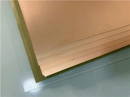
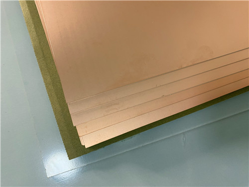
Может быть поставлен сырой ламинат TMM10i. Могут быть изготовлены полностью готовые 2-слойные ВЧ печатные платы с покрытием ENIG и краевым покрытием.
Свяжитесь с нами сегодня для:
Предоставления образцов материала и проведения испытаний
Помощи в проектировании ВЧ схем
Расчета импеданса и поддержки проектирования
Расчета стоимости печатных плат и обзора DFM
Технической поддержки для вашего конкретного применения
Впишите ваше сообщение

RO4350B, 4003C; Rogers 5880, 5870, 6002, 6010, 6006, 6035; RO3003, RO3035, RO3006, RO3010, RO3210, RO3203
TLX-8, TLX-6, TLX-9, TLX-0, TLX-7, TLY-3, TLY-5, RF-35TC, RF-60TC, RF-35A2, RF-60A, AD450, AD600, TMM4, TC350
| Shenzhen Bicheng Electronics Technology Co., Ltd |
| городок 6-11К Шидай Джингюан Фуйонг, район Баоан, город Шэньчжэня, провинция Гуандун, Китай |
| 86-755-27374946 |
| sales30@bichengpcb.com |